
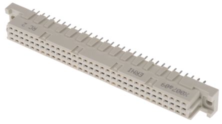
Description
The 64-way ‘EuroConnector’ is a DIN 41612/IEC 60603-2 Type-C Connector and the standard expansion port for peripherals.
The single connector can be extended with a SamBus or a Two-up or Three-up.
Pin Out:
(NB row A is at the bottom of the Euroconnector, row C at the top).
| PIN | SIGNAL | PIN | SIGNAL |
|---|---|---|---|
| 1A | DBDIR | 1C | IORQL |
| 2A | RDL | 2C | MREQL |
| 3A | WRL | 3C | HALTL |
| 4A | BUSAKL | 4C | NMIL |
| 5A | WAITL | 5C | INTL |
| 6A | BUSREQL | 6C | CD1 |
| 7A | RESETL | 7C | CDO |
| 8A | CM1L | 8C | CD7 |
| 9A | REFRESHL | 9C | CD2 |
| 10A | 0 VOLTS | 1OC | +5 VOLTS |
| 11A | AO | 11C | CD6 |
| 12A | A1 | 12C | CD5 |
| 13A | A2 | 13C | CD3 |
| 14A | A3 | 14C | CD4 |
| 15A | A4 | 15C | CPU CLK |
| 16A | A5 | 16C | A15 |
| 17A | A6 | 17C | A14 |
| 18A | A7 | 18C | A13 |
| 19A | A8 | 19C | A12 |
| 20A | A9 | 20C | All |
| 21A | A10 | 21C | DISK 2L |
| 22A | MSEINTL | 22C | ROMCSL |
| 23A | XMEML | 23C | EARMIC |
| 24A | 8 MHz | 24C | DISK 1L |
| 25A | RED 1 | 25C | PRINTL |
| 26A | GREEN 1 | 26C | BLUE 1 |
| 27A | C SYNC | 27C | ROMCSRL |
| 28A | SPEN | 28C | AUDIO RIGHT OUTPUT |
| 29A | BLUE 0 | 29C | AUDIO LEFT OUTPUT |
| 30A | RED 0 | 30C | COMP VIDEO |
| 31A | BRIGHT | 31C | GREEN 0 |
| 32A | +5 VOLTS | 32C | 0 VOLTS |
Line Detail:
| Line | Description |
|---|---|
| DBDIR (1A) | This signal is not used by the computer but must be driven by all external devices to allow their use with the SME. The SME has buffers present to prevent undue loading of the machine. However, it is the responsibility of the hardware designer to ensure that the data bus transceiver has its direction bit set according to the operation (read or write) being performed. The operation should be as follows: 1. Processor sends out an address. 2. External device decodes address. 3. External device drives the DBDIR line, from an open collector output, LOW for a processor READ. It is configured as a WIRED-OR internally to the computer. 4. Normal handshaking is continued with the Z80B for data tranfser. |
| RDL (2A) | Read signal from the processor. |
| WRL (3A) | Write signal from the processor. |
| BUSAKL (4A) | Bus acknowledge signal from the processor. |
| WAITL (5A) | Wait signal to processor. |
| BUSREQL (6A) | Bus request signal to external device. |
| RESETL (7A) | This is a system reset generated by a 10 Kilohm resistor charging a 47 microfarad capacitor. This gives a pulse of approximately 330ms duration. It is suggested that if a sharp reset edge is required, this signal is passed through a Schmitt inverter. |
| CM1L (8A) | Op-code fetch signal from the processor. |
| REFRESHL (9A) | Refresh signal from the processor. |
| 0 V (10A) | Zero Volt: not to be used as a supply rail. |
| AO (11A) | Address lines AO to A10 from the processor are on pins 11A to 21A. |
| MSEINTL (22A) | Mouse interrupt signal also present on the mouse port. The signal is pulled low by an external device to notify the processor that the mouse co-ordinates have changed. |
| XMEML (23A) | External memory signal which will be driven low when the processor requires to switch out the internal memory and access the external memory. Please note that only memory above address 8000H in each block of 64K will be switched out. It is the responsibility of the peripheral designer to ensure that the XMEM signal is included in the address decoding circuitry of the design, to avoid contention between the internal RAM and the external device. |
| BMHZ (24A) | 8 MegaHertz clock signal. |
| RED1 (25A) | Each colour is generated by three colour driver signals, the intensity of which is determined by three bits each. RED1 is the MSB (Most Significant Bit) of the red colour signal at the current pixel position. |
| GREEN1 (26A) | GREEN1 is the MS B of the green colour signal (see pin 25A for a full description). |
| CSYNC (27A) | Composite Sync for video circuitry as on the SCART connector. |
| SPEN (28A) | Light pen signal (active high) which is normally low. When the light pen is touched to the screen and the raster passes the point of the pen, a positive going edge is received on this signal from the light pen socket. This causes the two registers LPEN and HPEN to contain the current x and y co-ordinates of the light pen, respectively. |
| BLUEO (29A) | BLUE0 is the second bit of the blue colour signal (see pin 25A for a full description). |
| REDO (30A) | REDO is the second bit of the red colour signal (see pin 25A for a full description). |
| BRIGHT (31A) | BRIGHT is the LSB (Least Significant Bit) of all colour signals (see pin 25A for a full description). |
| +5V (32A) | +5 Volt supply rail, up to 250 mA available. |
| IORQL (1C) | Input/Output Request becomes active when the address bus contains a current port address from the processor. |
| MREQL (2C) | Memory Request becomes active when the address bus contains a current memory address from the processor. |
| HAUL (3C) | Halt indicates from the processor that it has executed a HALT instruction and is waiting for an interrupt. |
| NMIL (4C) | Non Maskable Interrupt causes the processor to execute a jump, from which it may be vectored anywhere by the user. It is used as a BREAK button by BASIC, and a SNAPSHOT button by the DOS. It is pulled up by a 10 Kilohm resistor internally, and should therefore be driven low by an open collector circuit. |
| INTL (5C) | Maskable Interrupt is used to interrupt the processor from its current task if the interrupts are currently enabled. |
| CD1 (6C) | Data lines D1,DO,D7 and D2 are on pins 6C to 9C. |
| +5V (1OC) | +5 Volt reference only. |
| CD6 (11C) | Data lines D6,D5,D3 and D4 are on pins 11C to 14C. |
| CPUCLK (15C) | The 6 MegaHertz clock signal to the processor. |
| A15 (16C) | Address lines A15 to All are on pins 16C to 20C. |
| DISK2L (21C) | DISK2 is the decoded base address for the eight ports of drive 2. |
| ROMCSL (22C) | ROM chip select is pulled high to disable the internal ROM (Used in conjunction with ROMCSR on pin 27C). It indicates when the ROM is being accessed. |
| EARMIC (23C) | EARMIC is connected to the logic level side of the cassette port circuitry. |
| DISK1L (24C) | DISK1 is the decoded base address for the eight ports of drive 1. |
| PRINTL (25C) | PRINT is the decoded address for either of the two possible printer addresses (246 and 248). |
| BLUE1 (26C) | BLUE1 is the MSB of the blue colour signal (see pin 25A for a full description). |
| ROMCSRL (27C) | ROMCSR is connected to the ROMCS (22C) pin via a 1 Kilohm resistor. If ROMCS is pulled high by an external circuit, then ROMCSR could be used as a chip select for an external ROM which would then take the place on the internal one. |
| AUDIORIGHT (28C) | The right audio signal, as on the light pen socket, is brought out here.(50mV pp as per auxiliary standard input) It must be amplified before being applied to a speaker. |
| AUDIOLEFT (29C) | The left audio signal is present on this pin. The same precautions and signal levels as for AUDIORIGHT apply. |
| CVID (30C) | Composite Video, as sent to the modulator and SCART socket is present on this pin. |
| GREEN0 (31C) | GREEN0 is the second bit of the green colour signal (see pin 25A for a full description). |
| 0 V (32C) | Zero Volt supply rail. |